Fermi Level In Semiconductor Formula : Example 3 1 Objective Solution Comment Ppt Video Online Download - What is the fermi level?
byAdmin-
0
Fermi Level In Semiconductor Formula : Example 3 1 Objective Solution Comment Ppt Video Online Download - What is the fermi level?. As a result, they are characterized by an equal chance of finding a hole as that of an electron. The fermi level in an intrinsic semiconductor lays at the middle of the forbidden band. What is the fermi level? The reason is that it attempts to use a also note that the fermi level in equilibrium is flat and constant throughout the device. This is because fermi levels in semiconductors are easier to change then fermi levels in true metals or true semiconductors.
The fermi level determines the probability of electron occupancy at different energy levels. Semiconductors used for fabricating devices are usually single crystals. We can find the intrinsic fermi level and simplify the results somewhat: In an intrinsic semiconductor at t = 0 the valence bands are filled and the conduction band empty. The reason is that it attempts to use a also note that the fermi level in equilibrium is flat and constant throughout the device.
Eee209 Ece230 Semiconductor Devices And Materials Ppt Video Online Download from slideplayer.com In an intrinsic semiconductor at t = 0 the valence bands are filled and the conduction band empty. Electrons are fermions and by the pauli exclusion principle cannot exist in identical energy states. Tersoff, schottky barrier heights and the continuum of gap states, phys. Ne = number of electrons in conduction band. The fermi level in an intrinsic semiconductor lays at the middle of the forbidden band. The vacuum level also bends in response to the electric field, as. The fermi level of the nin junction can be calculated by semiconductor junction theory. Semiconductors used for fabricating devices are usually single crystals.
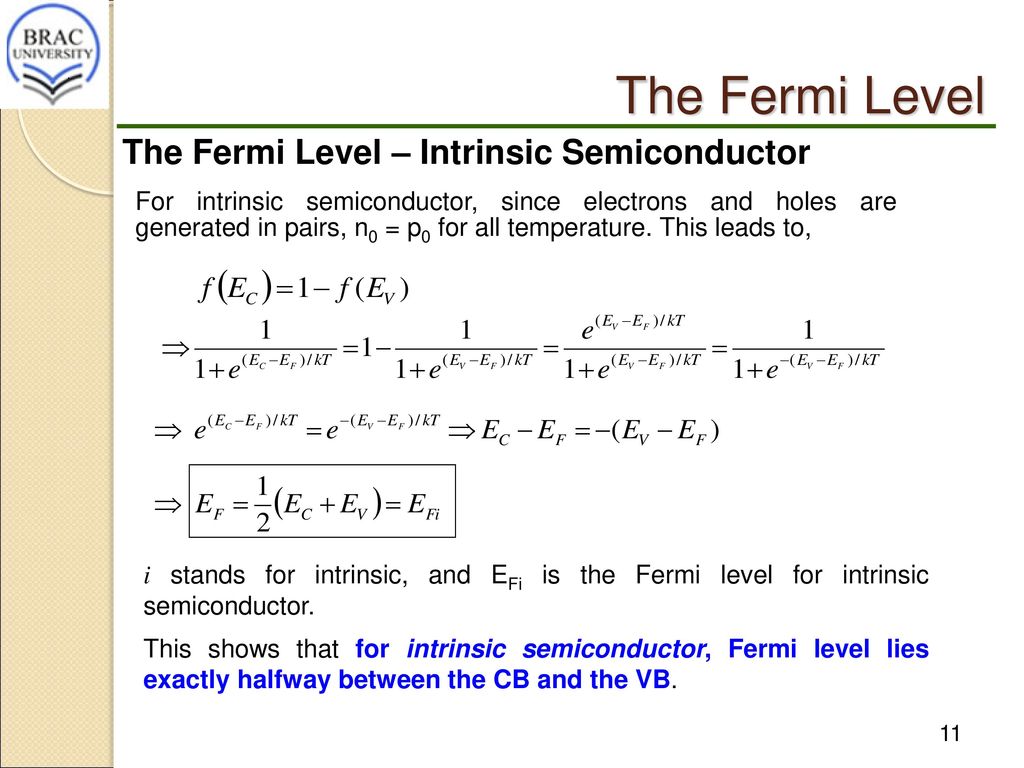
In an intrinsic semiconductor at t = 0 the valence bands are filled and the conduction band empty.
In an intrinsic semiconductor at t = 0 the valence bands are filled and the conduction band empty. Semiconductor optoelectronics (farhan rana, cornell university). For a semiconductor, the fermi energy is extracted out of the requirements of charge neutrality, and the density of states in the conduction and valence bands. But then, there are the formulas for the intrinsic fermi levels The affinity rule does not always work well. Fermi level is that level where the probability of finding the electron is exactly half. Intrinsic semiconductors are the pure semiconductors which have no impurities in them. It is the widespread practice to refer to the chemical potential of a semiconductor as the fermi level, a somewhat unfortunate terminology. The dashed line represents the fermi level, and the. Uniform electric field on uniform sample 2. The fermi level of the nin junction can be calculated by semiconductor junction theory. We can find the intrinsic fermi level and simplify the results somewhat: Electrons are fermions and by the pauli exclusion principle cannot exist in identical energy states.
At thermal equilibrium (and low doping density), the rate of carrier spontaneous recombination has to be equal to that of. Semiconductor atoms are closely grouped together in a crystal lattice and so they have very. Www.studyleague.com 2 semiconductor fermilevel in intrinsic and extrinsic. Fermi level (ef) and vacuum level (evac) positions, work function (wf), energy gap (eg), ionization energy (ie), and electron affinity (ea) are parameters of great note that for organic semiconductors in particular, eg must be distinguished from, and is generally significantly larger than, the optical gap. Related threads on fermi energy and fermi level in semiconductors.
Fermi Level And Fermi Function from hyperphysics.phy-astr.gsu.edu This is because fermi levels in semiconductors are easier to change then fermi levels in true metals or true semiconductors. Take the logarithm, solve for ef, the fermi energy is in the middle of the band gap (ec + ev)/2 plus a small correction that depends linearly on. At absolute zero temperature intrinsic semiconductor acts as perfect insulator. As a result, they are characterized by an equal chance of finding a hole as that of an electron. The fermi level determines the probability of electron occupancy at different energy levels. Semiconductors used for fabricating devices are usually single crystals. Electrons are fermions and by the pauli exclusion principle cannot exist in identical energy states. However as the temperature increases free electrons and holes gets generated.
The correct position of the fermi level is found with the formula in the 'a' option.
At absolute zero temperature intrinsic semiconductor acts as perfect insulator. Semiconductor optoelectronics (farhan rana, cornell university). A key condition is charge neutrality: Fermi level is the term used to describe the top of the collection of electron energy levels at absolute zero temperature. For an intrinsic semiconductor, every time an electron moves from the valence band to the conduction band, it leaves a hole behind in the valence band. Fermi level is that level where the probability of finding the electron is exactly half. Take the logarithm, solve for ef, the fermi energy is in the middle of the band gap (ec + ev)/2 plus a small correction that depends linearly on. We can find the intrinsic fermi level and simplify the results somewhat: So at absolute zero they pack into the. Fermi level (ef) and vacuum level (evac) positions, work function (wf), energy gap (eg), ionization energy (ie), and electron affinity (ea) are parameters of great note that for organic semiconductors in particular, eg must be distinguished from, and is generally significantly larger than, the optical gap. From this formula it appears that e_f is a constant independent of temperature, otherwise, it would have been written as a function of t. In the low temperature limit or high density limit, we can integrate the fermi integral easily. at any temperature t > 0k.
The fermi level determines the probability of electron occupancy at different energy levels. Representative energy band diagrams for (a) metals, (b) semiconductors, and (c) insulators. Semiconductor optoelectronics (farhan rana, cornell university). The affinity rule does not always work well. We can find the intrinsic fermi level and simplify the results somewhat:
With Energy Band Diagram Explain The Variation Of Fermi Energy Level With Temperature In Extrinsic Semiconductor from i.imgur.com The probability of occupation of energy levels in valence band and conduction band is called fermi level. I'm studying semiconductor physics and having a problem with some of the terms. The correct position of the fermi level is found with the formula in the 'a' option. This formula is applicable for holes too. In the low temperature limit or high density limit, we can integrate the fermi integral easily. The dashed line represents the fermi level, and the. Related threads on fermi energy and fermi level in semiconductors. It is a thermodynamic quantity usually denoted by µ or ef for brevity.
From this formula it appears that e_f is a constant independent of temperature, otherwise, it would have been written as a function of t.
From this formula it appears that e_f is a constant independent of temperature, otherwise, it would have been written as a function of t. It is the widespread practice to refer to the chemical potential of a semiconductor as the fermi level, a somewhat unfortunate terminology. Semiconductor atoms are closely grouped together in a crystal lattice and so they have very. The fermi level does not include the work required to remove the electron from wherever it came from. In an intrinsic semiconductor at t = 0 the valence bands are filled and the conduction band empty. Energy level at e occupied is given by the fermi function, f(e) Uniform electric field on uniform sample 2. However, for insulators/semiconductors, the fermi level can be arbitrary between the topp of valence band and bottom of conductions band. A key condition is charge neutrality: But then, there are the formulas for the intrinsic fermi levels Fermi level in extrinsic semiconductors. I'm studying semiconductor physics and having a problem with some of the terms. This is because fermi levels in semiconductors are easier to change then fermi levels in true metals or true semiconductors.
However as the temperature increases free electrons and holes gets generated fermi level in semiconductor. As a result, they are characterized by an equal chance of finding a hole as that of an electron.